- 您现在的位置:买卖IC网 > Sheet目录480 > MTD20P06HDLT4 (ON Semiconductor)MOSFET P-CH 60V 15A DPAK
MTD20P06HDL
Preferred Device
Power MOSFET
20 Amps, 60 Volts, Logic
Level
P?Channel DPAK
This Power MOSFET is designed to withstand high energy in the
avalanche and commutation modes. The energy efficient design also
offers a drain?to?source diode with a fast recovery time. Designed for
low?voltage, high?speed switching applications in power supplies,
converters and PWM motor controls, and other inductive loads. The
avalanche energy capability is specified to eliminate the guesswork in
designs where inductive loads are switched, and to offer additional
safety margin against unexpected voltage transients.
http://onsemi.com
20 AMPERES, 60 VOLTS
R DS(on) = 175 m W
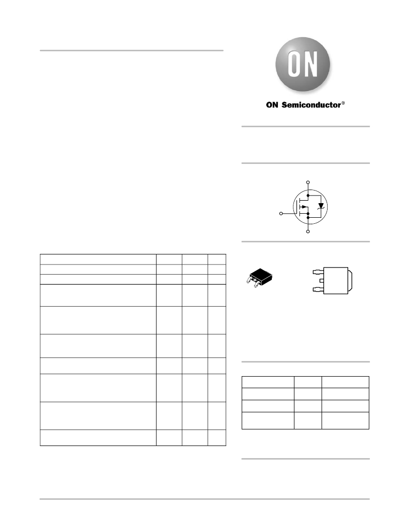
P?Channel
D
Features
? Ultra Low R DS(on) , High?Cell Density, HDTMOS
? Diode is Characterized for Use in Bridge Circuits
? I DSS and V DS(on) Specified at Elevated Temperature
? Avalanche Energy Specified
? Pb?Free Package is Available
G
S
MAXIMUM RATINGS (T C = 25 ° C unless otherwise noted)
MARKING DIAGRAM & PIN ASSIGNMENTS
Rating
Symbol
Value
Unit
Drain?Source Voltage
Drain?Gate Voltage (R GS = 1.0 M W )
Gate?Source Voltage
? Continuous
? Non?Repetitive (t p v 10 ms)
V DSS
V DGR
V GS
V GSM
60
60
" 15
" 20
Vdc
Vdc
Vdc
Vpk
1 2
3
4
DPAK
CASE 369C
Gate 1
Drain 2
Source 3
YWW
20P
06HLG
4
Drain
Drain Current
? Continuous
? Continuous @ 100 ° C
? Single Pulse (t p v 10 m s)
I D
I D
I DM
15
9.0
45
Adc
Apk
(Surface Mount)
STYLE 2
20P06HL = Device Code
Total Power Dissipation
Derate above 25 ° C
Total Power Dissipation @ T C = 25 ° C (Note 2)
Operating and Storage Temperature Range
P D
T J , T stg
72
0.58
1.75
?55 to
W
W/ ° C
W
° C
Y
WW
G
= Year
= Work Week
= Pb?Free Package
150
ORDERING INFORMATION
Single Pulse Drain?to?Source Avalanche
Energy ? Starting T J = 25 ° C
E AS
300
mJ
Device
Package
Shipping ?
(V DD = 25 Vdc, V GS = 5.0 Vdc,
I L = 15 Apk, L = 2.7 mH, R G = 25 W )
MTD20P06HDL
DPAK
75 Units/Rail
Thermal Resistance
° C/W
MTD20P06HDLT4
DPAK
2500 Tape & Reel
? Junction?to?Case
? Junction?to?Ambient (Note 1)
? Junction?to?Ambient (Note 2)
R q JC
R q JA
R q JA
1.73
100
71.4
MTD20P06HDLT4G
DPAK
(Pb?Free)
2500 Tape & Reel
Maximum Lead Temperature for Soldering T L 260 ° C
Purposes, 1/8 ″ from case for 10 seconds
Stresses exceeding Maximum Ratings may damage the device. Maximum
Ratings are stress ratings only. Functional operation above the Recommended
Operating Conditions is not implied. Extended exposure to stresses above the
Recommended Operating Conditions may affect device reliability.
1. When surface mounted to an FR4 board using the minimum recommended
pad size.
2. When surface mounted to an FR4 board using 0.5 sq. inch pad size.
?For information on tape and reel specifications,
including part orientation and tape sizes, please
refer to our Tape and Reel Packaging Specification
Brochure, BRD8011/D.
Preferred devices are recommended choices for future use
and best overall value.
? Semiconductor Components Industries, LLC, 2006
June, 2006 ? Rev. 6
1
Publication Order Number:
MTD20P06HDL/D
发布紧急采购,3分钟左右您将得到回复。
相关PDF资料
MTD2955VT4
MOSFET P-CH 60V 12A DPAK
MTD3010N
PHOTO DIODE 900NM DOME CLR TO-18
MTD3010PM
PHOTO DIODE 900NM DOME CLR TO-18
MTD3055VL
MOSFET N-CH 60V 12A DPAK
MTD3055V
MOSFET N-CH 60V 12A DPAK
MTD5010N
PHOTO DIODE 850NM DOME CLR TO-18
MTD5010W
PHOTO DIODE 850NM FLAT CLR TO-18
MTD5052N
PHOTO DIODE 525NM B/G CLR TO-18
相关代理商/技术参数
MTD214
制造商:未知厂家 制造商全称:未知厂家 功能描述:Ethernet Encoder/Decoder and 10BaseT Transceiver with Built-in Waveform Shaper
MTD2525J
制造商:SHINDENGEN 制造商全称:Shindengen Electric Mfg.Co.Ltd 功能描述:DMOS Microstepping Dual PWM Motor Driver
MTD2955E
制造商:MOTOROLA 制造商全称:Motorola, Inc 功能描述:TMOS POWER FET 12 AMPERES 60 VOLTS RDS(on) = 0.3 OHM
MTD2955ET4
制造商:Motorola Inc 功能描述:
MTD2955V
功能描述:MOSFET DISC BY MFG 2/02
RoHS:否 制造商:STMicroelectronics 晶体管极性:N-Channel 汲极/源极击穿电压:650 V 闸/源击穿电压:25 V 漏极连续电流:130 A 电阻汲极/源极 RDS(导通):0.014 Ohms 配置:Single 最大工作温度: 安装风格:Through Hole 封装 / 箱体:Max247 封装:Tube
MTD2955V1
制造商:ON Semiconductor 功能描述:Trans MOSFET P-CH 60V 12A 3-Pin(3+Tab) IPAK Rail
MTD2955V-1
制造商:ONSEMI 制造商全称:ON Semiconductor 功能描述:Power MOSFET 12A, 60V P-Channel DPAK
MTD2955V-1G
制造商:ONSEMI 制造商全称:ON Semiconductor 功能描述:Power MOSFET 12A, 60V P-Channel DPAK
